Last Updated on April 3, 2026 by Hemanth
Table of Contents
Gallium is one of those elements that quietly runs the modern world. It’s inside the high-frequency chips that make 5G possible, the LEDs that light our homes, and the solar cells that power satellites. In liquid form, it even cools advanced electronics and enables the rise of soft, flexible machines.
In this article, you’ll uncover how gallium supports semiconductors, batteries, aerospace systems, and next-gen electronics. More than just a supporting metal, it’s recognized globally as a critical mineral — one that links technology, clean energy, and national security in ways most people never realize.
Overview
The same metal that keeps your phone connected to Wi-Fi also helps spacecraft survive the extremes of space. Gallium melts at just 29.76 °C — warm enough to liquefy in your hand — yet performs flawlessly in electronics operating hundreds of degrees hotter.
What are the uses of gallium? Gallium is used in gallium arsenide (GaAs) and gallium nitride (GaN) semiconductors for high-frequency and power electronics, CIGS thin-film solar cells, LEDs, laser diodes, high-performance cooling systems, and medical imaging isotopes. Gallium alloys also enable flexible electronics, soft robotics, and liquid-metal circuits.
Researchers have even printed gallium-based circuits directly onto human skin like temporary tattoos, creating wearable sensors that can stretch, bend, and still conduct electricity — opening entirely new categories of medical and consumer devices.
Production is led by China, Russia, and Germany, with demand concentrated in telecom, renewable energy, defence, and advanced manufacturing.
This guide explores the most important gallium uses across electronics, energy, medicine, and emerging technologies — showing how one low-melting metal enables some of the world’s most advanced systems.
Elemental Profile: What Makes Gallium Unique

Gallium’s discovery stands as one of science’s most remarkable validations of theoretical prediction. In 1871, Russian chemist Dmitri Mendeleev identified a gap in his periodic table and predicted an undiscovered element he termed “eka-aluminium”. His calculations proved extraordinarily precise—anticipating atomic weight, density, and melting point within striking accuracy of the actual element.
Four years later, French chemist Paul-Émile Lecoq de Boisbaudran spotted gallium through spectroscopy, detecting two distinct violet lines at wavelengths of 4170 and 4031 angstroms in sphalerite samples.
From 52 kg of mineral ore, he extracted mere milligrammes of gallium chloride, then isolated over one gramme of nearly pure metal through electrolysis. Lecoq chose “gallium” from the Latin Gallia, meaning Gaul, honouring his homeland.
From Theory to Reality: Mendeleev’s Vindication
Lecoq’s achievement provided powerful evidence for Mendeleev’s periodic table framework. Starting with just 600mg extracted from 450 kilos of ore, Lecoq eventually produced 75 grammes of gallium from more than 4 tonnes of raw material. His measured atomic mass of 69.86 came remarkably close to today’s accepted value of 69.723.
Physical Properties: The Liquid Metal Paradox
Gallium (chemical symbol Ga, atomic number 31) exhibits properties that seem to defy conventional expectations. Its characteristics create unique opportunities across multiple industrial sectors.
| Property | Measurement | Strategic Importance |
|---|---|---|
| Melting point | 29.76°C | Liquid at body temperature |
| Boiling point | ~2400°C | Widest liquid range of any element |
| Thermal expansion | 3.10% upon solidification | Requires specialised container design |
| Surface tension | 10× that of water | Voltage-controllable in ionic solutions |
| Density | 5.91 g/cm³ | Comparable to heavy metals like bismuth |
> Material Insight: Gallium contracts as it melts (like water), causing solid gallium to float on its liquid form—a property shared only with bismuth and antimony.
Chemical Behaviour: Amphoteric Reactivity and Oxide Formation
Gallium demonstrates unusual chemical versatility. Stable in dry air, it rapidly forms a protective gallium oxide film (Ga₂O₃) when exposed to oxygen or moisture. This oxide “skin” provides liquid gallium with structural rigidity, enabling it to hold complex shapes essential for flexible electronic applications.
The element exhibits amphoteric behaviour—reacting with both acids and bases. Contact with sodium and potassium hydroxide solutions produces gallates and hydrogen gas. Gallium typically adopts the +3 oxidation state, though +1 states occasionally occur.
Properties Enable Applications: The Connection Matrix
Gallium’s distinct properties directly unlock specific technological capabilities:
- Body-temperature melting: Enables mercury-free thermometers and thermal interfaces
- Controllable oxide skin: Allows precise patterning in flexible circuits and skin electronics
- Exceptional liquid range: Supports high-temperature heat transfer in extreme environments
- Shape memory behaviour: Powers self-repairing circuits that reconnect after damage
- Minimal toxicity: Permits medical and consumer uses impossible with mercury alternatives
Key Takeaway: Gallium combines theoretical elegance with practical utility—its predicted properties creating a material perfectly suited for applications spanning electronics, thermal management, and biomedical technology.
What Makes Gallium Essential for Electronics
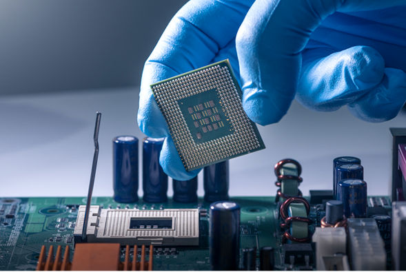
Image Source: Metal Tech News
Gallium (chemical symbol Ga, atomic number 31) may occupy a modest position on the periodic table, but its electronic properties pack extraordinary punch. Three fundamental characteristics separate this element from conventional metals, creating capabilities that traditional materials simply cannot match.
Mercury’s Safer Replacement: Low Toxicity with Superior Performance
For decades, mercury dominated applications requiring liquid metals despite well-documented health hazards. Studies comparing transport system effects show that whilst both mercury and gallium ions influence biological processes, gallium demonstrates substantially lower toxicity.
This safety margin enables gallium’s use in medical thermometers, diagnostic imaging, and consumer electronics where human contact occurs. The environmental comparison reveals stark differences:
| Property | Gallium | Mercury |
|---|---|---|
| Toxicity level | Low | High |
| Vapour emission | Minimal | Significant |
| Environmental persistence | Lower | Higher |
| Safe handling requirements | Standard | Extensive |
Consequently, gallium alloys have become the preferred choice for medical devices and electronics manufacturers prioritising worker safety and environmental responsibility.
While elemental gallium is generally considered low-toxicity for casual handling, certain compounds — particularly gallium arsenide (GaAs) and gallium nitride (GaN) — can release hazardous particulates during machining, recycling, or high-temperature processing, making dust-control measures and PPE essential.
Gallium also causes rapid embrittlement of aluminium and aggressively wets many metals; in cooling systems and liquid-metal applications, protective coatings such as nickel/gold (Ni/Au) or polymers are recommended, and dissimilar metals should be isolated to minimise galvanic corrosion.
The numbers reveal GaAs’s dominance: it powers the communications infrastructure we depend on daily, from mobile phone networks to satellite systems and military radar installations. Unlike silicon components, GaAs generates significantly less noise at high frequencies whilst supporting higher collapse voltages — critical advantages for telecommunications infrastructure, aerospace applications, and defence systems.
Historically, most primary gallium fed gallium arsenide (GaAs); today, GaAs and gallium nitride (GaN) together account for the majority of end-use, with GaAs still dominant in high-frequency and infrared systems and GaN growing rapidly across 5G, EV power electronics, and defence applications.
Surface Engineering at the Molecular Level
Gallium’s surface tension—approximately ten times higher than water—creates unique manufacturing possibilities. When exposed to air or moisture, the metal forms a protective gallium oxide “nano-skin” with remarkable control characteristics. This oxide layer demonstrates several critical properties:
- Self-passivates the underlying metal surface
- Enables precise microstructure formation
- Bonds effectively to diverse substrate materials
- Responds predictably to chemical and electrochemical manipulation
The surface tension of this oxide skin measures consistently between 350–365 mN/m across different substrate surfaces and gallium alloy compositions. This predictability allows engineers to pattern and mould liquid metal components with precision previously impossible in flexible electronics.
Thermal Stability Across Extreme Ranges
No other element matches gallium’s liquid temperature span of approximately 2,000°C—from 29.76°C melting point to roughly 2,400°C boiling point [37,38]. This unprecedented range creates thermal stability advantages that materials scientists describe as transformative.
> Technical insight: Gallium’s boiling point exceeds its melting point by nearly nine times on the absolute temperature scale—the highest ratio among all elements.
Unlike mercury and other liquid metals, gallium maintains negligible vapour pressure up to 1,500°C, eliminating toxic emission concerns during high-temperature processing. These thermal characteristics enable applications in extreme environments where other liquid metals would vaporise or decompose.
Key Takeaway: Gallium combines safety, surface controllability, and thermal range in ways no other liquid metal can achieve—enabling electronics that bend, heal, and operate across temperature extremes impossible with conventional materials.
From semiconductors to renewable energy, the uses of gallium directly trace back to its unusual physical and chemical profile.
Gallium Compound Electronics & Semiconductors
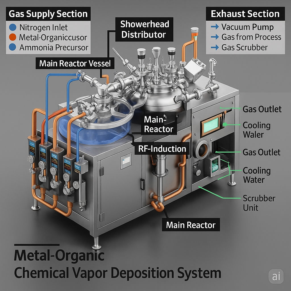
Gallium’s true power lies not in its pure form, but in its compounds — materials that have quietly enabled the most demanding applications in modern electronics. These semiconductor compounds possess electrical properties that silicon simply cannot match, creating possibilities that extend far beyond conventional computing.
Gallium Arsenide (GaAs): The Foundation of High-Speed Communications
Among the most critical gallium uses, gallium arsenide stands as the workhorse of high-frequency, a black-grey crystalline material with a melting point of 1,238°C that represents approximately 95% of global gallium consumption. Its sphalerite-type lattice structure features a lattice constant of 5.65 × 10⁻¹⁰m and a forbidden band width of 1.4 eV — specifications that translate directly into superior performance above 250 GHz.
The numbers reveal GaAs’s dominance: it powers the communications infrastructure we depend on daily, from mobile phone networks to satellite systems and military radar installations. Unlike silicon components, GaAs generates significantly less noise at high frequencies whilst supporting higher collapse voltages — critical advantages for telecommunications infrastructure, aerospace applications, and defence systems.
What makes this compound indispensable is its electron mobility, which far exceeds silicon’s capabilities. This property enables faster switching speeds and more efficient signal transmission, explaining why GaAs dominates microwave point-to-point links and radar systems where performance cannot be compromised.
Gallium Nitride (GaN): Powering the Next Generation
Gallium nitride represents a fundamental leap in semiconductor capability, featuring a hexagonal close-packed crystal structure that delivers extraordinary power efficiency. Its wide bandgap, strong atomic bonds, and exceptional thermal conductivity make it the material of choice for applications where silicon fails.
Defence applications showcase GaN’s advantages most clearly:
- Power conversion efficiency exceeding conventional alternatives
- Dramatic size and weight reductions
- Broader operational bandwidth
- Exceptional durability under extreme conditions
These properties make GaN essential for electronic warfare systems, including jammers requiring high power output across wide frequency ranges. The same characteristics that enable military applications also drive GaN’s critical role in 5G infrastructure and advanced radar systems.
While GaN is rapidly becoming the material of choice for high-efficiency devices in power electronics, it exists within a competitive landscape of wide bandgap semiconductors. Engineers often weigh GaN’s performance not just against legacy silicon, but also against established SiC devices and the emerging ultra-wide bandgap contender, β-Ga₂O₃ — each with distinct semiconductor materials advantages.
The table below compares these four platforms across key metrics relevant to power device design:
Performance Comparison: GaN, SiC, Si, and Ga₂O₃ in Power Electronics
| Property | Silicon (Si) | Silicon Carbide (SiC) | Gallium Nitride (GaN) | Gallium Oxide (Ga₂O₃) | Strategic Advantage |
| Bandgap (eV) | 1.1 | 3.3 | 3.4 | 4.5–5.1 | Ga₂O₃ |
| Breakdown Field (MV/cm) | 0.3 | 3.0 | 3.3 | 8.0 | Ga₂O₃ |
| Electron Mobility (cm²/V·s) | ~1500 | ~900 | ~2000 | ~300 | GaN |
| Thermal Conductivity (W/m·K) | 150 | 120–490 | 130–230 | 10–27 | SiC |
| Max Junction Temperature (°C) | 150 | 200 | 200+ | TBD* | SiC / GaN |
| Cost Trend | Low | Medium | Medium-High | High | Si |
*TBD: Limited by thermal management solutions due to low κ; substrate engineering in progress.
Gallium arsenide remains one of the most significant gallium uses, forming the backbone of military radar, satellite communication, and high-speed data links.
Case Study – AESA radar
- Company/Project: Raytheon’s AN/APG-79 AESA radar
- Challenge: Improve range and resistance to electronic countermeasures
- Gallium Solution: GaN-based transmit/receive modules replaced legacy GaAs modules
- Results: 40% range increase, higher reliability, reduced cooling load
- Source: [Raytheon Defence Systems]
Case Study – Telecom: 5G Base Station PA
- Company/Project: NTT Docomo 5G rollout
- Challenge: Reduce size and power consumption in massive MIMO base stations
- Gallium Solution: GaN high-electron-mobility transistors (HEMTs) in power amplifiers
- Results: 25% energy savings, smaller enclosures
- Source: [NTT Docomo Technical Journal]
Key Takeaway: GaN and SiC dominate current wide bandgap applications, with Ga₂O₃ emerging as a next-generation contender for ultra-high-voltage devices. Silicon remains cost-effective for legacy and low-power uses, but cannot match the performance envelopes of these wide bandgap semiconductors.
Gallium Oxide (Ga₂O₃): Ultra-Wide Bandgap Pioneer
Gallium oxide pushes semiconductor performance into previously impossible territory with its ultra-wide bandgap spanning 4.5 eV to 5.16 eV (Higashiwaki et al., 2022) and a critical breakdown electrical field of 8 MV/cm (Zhao et al., 2023) — surpassing silicon, silicon carbide, and even gallium nitride. These extreme specifications translate into exceptional promise for power electronics and radio frequency applications.
Manufacturing breakthroughs now enable large-scale β-Ga₂O₃ single crystal substrates through floating zone, edge-defined film-fed growth, and Czochralski techniques. The results speak for themselves: planar Ga₂O₃ transistors achieving breakdown electric fields of 8 kV, pushing performance boundaries that seemed theoretical just years ago.
Most research targets the β-phase due to its stability and ultra-wide bandgap. Wafer diameters currently range from 2 to 4 inches (Higashiwaki et al., 2022), with thermal conductivity values as low as 10–27 W/m·K, creating hot-spot risks in high-power devices. To address these issues, engineers are experimenting with substrate engineering (e.g., diamond or SiC composites) and hybrid conduction paths in Schottky barrier diodes (SBD) and MOSFET architectures designed for high-voltage switching.
Performance Comparison: GaAs Against Silicon
| Property | GaAs | Silicon | Strategic Advantage |
| Electron mobility | Higher | Lower | GaAs |
| High-frequency noise | Lower | Higher | GaAs |
| Manufacturing cost | INR 2953315.78/m² | INR 8438.050/m² | Silicon |
| Solar efficiency | >28% | 15-20% | GaAs |
| Thermal tolerance | Superior | Limited | GaAs [153] |
The cost differential remains significant, but performance applications justify the premium. GaAs delivers electron mobility and thermal characteristics that silicon cannot approach, whilst generating substantially less noise at the high frequencies essential for modern communications.
Key Takeaway: GaN and SiC dominate current wide bandgap semiconductors, with Ga₂O₃ emerging as a next-generation contender for ultra-high-voltage devices. Silicon remains cost-effective for legacy and low-power uses, but cannot match the performance envelopes of these advanced platforms.
Gallium Applications Optoelectronics & Display Technologies

Image Source: Nature
The brilliant colours on your smartphone screen and the efficient LED bulbs illuminating your home share a common foundation: gallium compounds that convert electricity into precisely controlled light emission.
These materials enable the visual technologies that define modern life, from ultra-high-definition displays to energy-efficient lighting systems.
LEDs & Laser Diodes: GaN for blue/white, GaAs for infrared
Gallium nitride fundamentally changed lighting by enabling blue and white LEDs with external quantum efficiencies exceeding 60%. This capability allowed LEDs to compete directly with incandescent and fluorescent technologies across the entire visible spectrum. GaN’s 3.45 eV direct bandgap produces near-ultraviolet light at 364 nm, making it ideal for applications requiring short wavelengths.
GaN laser diodes operate across distinct spectral bands, each tailored for specific applications:
- Violet (405 nm): Powers fluorescence microscopy and photolithography systems
- Blue (445 nm): Enables high-resolution displays and precision copper welding
- Green (520 nm): Critical for underwater communication where blue-green light penetrates deepest
Gallium arsenide takes a different approach, excelling in infrared applications through its direct bandgap characteristics that make it particularly suitable for longer wavelengths. GaAs powers semiconductor lasers, high-efficiency solar cells, and sensitive photodetectors across telecommunications and sensing applications.
Display Backplanes: IGZO in OLED/LCD & advanced screens
Indium gallium zinc oxide emerged in 2004 as a breakthrough semiconductor for thin-film transistor backplanes. IGZO delivers several critical advantages over conventional amorphous silicon:
| Property | Benefit | Real-World Application |
|---|---|---|
| Higher mobility | Smaller transistors | Thinner display bezels |
| Faster switching speed | Higher frame rates | 4K and 8K resolution displays |
| Lower power consumption | Extended battery life | Mobile devices and laptops |
Compared to low-temperature polysilicon (LTPS), IGZO offers higher uniformity and lower leakage currents, making it ideal for large displays, while LTPS retains an edge in pixel density for small-format OLED panels. Many manufacturers now deploy hybrid backplane strategies to balance these strengths.
LG Display employs IGZO as the primary TFT technology for its white OLED television systems, whilst Samsung has adopted IGZO for quantum-dot OLED displays. This widespread adoption reflects IGZO’s ability to meet the demanding requirements of next-generation screen technologies.
Quantum Dot Integration: Colour tuning & efficiency gains
Gallium-based quantum dots offer exceptional colour purity through precise engineering at the nanoscale. AgInₓGa₁₋ₓS₂ quantum dots, when enhanced with gallium sulphide shells, produce intense green emissions with peaks tunable between 499-543 nm. These structures achieve photoluminescence quantum yields exceeding 50%.
Gallium phosphide quantum dots demonstrate controllable emissions spanning 400-520 nm with photoluminescence quantum yields reaching 35-40%. Their narrow emission bandwidth (FWHM of 75 nm) makes them exceptional candidates for colour conversion in advanced display systems.
The precision control stems from quantum confinement effects, where gallium-based quantum dots function as artificial atoms with electronically controllable states. This enables manufacturers to tune colour output with extraordinary accuracy whilst maintaining high efficiency.
Key Takeaway: Gallium compounds dominate modern optoelectronics by delivering superior light emission control, enabling displays that consume less energy whilst producing more vibrant colours and lighting systems that achieve unprecedented efficiency across the visible spectrum.
Solar Cell Innovations
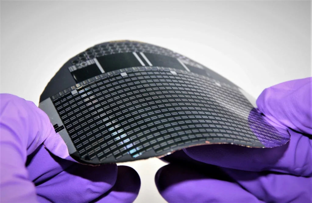
Image Source: Fraunhofer-Institut für Solare Energiesysteme ISE – Fraunhofer …
Gallium’s strategic importance extends beyond everyday electronics into renewable energy systems, where its compounds enable solar technologies that conventional silicon simply cannot match. These applications reveal gallium’s role in energy independence and next-generation photovoltaics.
CIGS Thin-Film Cells: Copper Indium Gallium Selenide for flexible PV
The bandgap tunability of Copper Indium Gallium Diselenide [Cu(InxGa1-x)Se2] creates opportunities impossible with fixed-bandgap materials. Adjusting gallium content shifts the bandgap from 1.04 eV for pure CIS to 1.68 eV for CGS, allowing precise optimisation for specific lighting conditions and applications.
The latest CIGS–perovskite tandem designs have achieved a certified conversion efficiency of 24.6%, as reported by Fraunhofer ISE in early 2025, marking a new benchmark for flexible photovoltaic technology. Commercial CIGS modules typically achieve 12–14% efficiency, making the technology a compelling alternative to traditional silicon in applications requiring flexibility.
The technology’s unique advantages include:
- Direct-bandgap absorption with minimal material thickness requirements
- Flexible substrate compatibility including glass, metal foils, and polymers
- Natural grain boundary passivation that prevents surface recombination
- Manufacturing flexibility through co-evaporation or precursor reaction processes, providing pathways for cost reduction and scaling.
Together, these advancements cement solar energy as one of the fastest-growing gallium uses in renewable technology
GaAs Solar Cells: High-efficiency space-grade photovoltaics
Gallium arsenide (GaAs) cells are prized in aerospace and concentrated photovoltaic (CPV) systems for their unmatched combination of efficiency, radiation resistance, and thermal stability. Space-grade stacks often pair GaAs with germanium substrates to maximize performance.
GaAs’s direct bandgap and high absorption coefficient enable it to deliver superior performance under intense sunlight and high-radiation conditions — qualities critical for satellites, space probes, and high-altitude drones.
Laboratory single-junction GaAs cells continue to hold world-class efficiency records of ~29.1%, based on pre-2020 results (e.g., Alta Devices), with no higher certified results reported by NREL as of 2025. Multi-junction GaAs-based cells achieve even greater efficiencies by stacking layers tuned to capture different parts of the solar spectrum, enabling performance levels above 30% in commercial space applications.
Gallium Doping in Silicon: Enhanced performance & longevity
Silicon solar cells gain substantial benefits from gallium doping, which addresses one of the technology’s persistent challenges: light-induced degradation. Gallium-doped silicon maintains stable carrier lifetime under illumination with minimal performance losses.
The shift from boron to gallium doping in monocrystalline PERC (Passivated Emitter and Rear Cell) production represents industry recognition of gallium’s superior properties. Research confirms that “as-received” gallium-doped Cz silicon achieves lifetimes comparable to specially treated boron-doped variants.
Higher-resistivity gallium-doped substrates (2-3 Ω cm) show potential for even greater cell efficiencies, suggesting continued opportunities for performance enhancement through gallium integration.
Key Takeaway: Gallium’s role in solar technology spans from flexible thin-films to record-breaking space cells and silicon enhancement, creating a strategic advantage in renewable energy systems where efficiency, durability, and performance stability determine commercial success.
Flexible Electronics & Wearables

Image Source: SciTechDaily
Electronics have always demanded that we adapt to their rigid, brittle constraints. Gallium changes this relationship entirely. This liquid metal creates circuits that bend, stretch, and conform to human skin — enabling electronics that adapt to us instead.
Stretchable Circuits: Embedded elastomers & flexible wiring
Liquid metal particles (LMPs) embedded within elastomers maintain electrical conductivity under mechanical stress that would destroy conventional circuits. These composites withstand stretching up to 400% without losing functionality. Recent advances include ligand-bound LMPs that prevent oxide layer growth, enabling one-step printing of stretchable circuits compared to conventional multi-step processes.
| Material Combination | Stretchability | Applications |
|---|---|---|
| EGaIn/PDMS | >300% | Wearable sensors |
| GaInSn/TPU | 100% | Biomonitoring |
| LB-LMPs/Polymer | 400% | Healthcare devices |
Self-Healing Circuits: Liquid metal flow & shape-memory recovery
Damage a traditional circuit, and it’s permanently broken. Damage a gallium circuit, and it repairs itself. When torn, the liquid metal simply flows back together when edges are repositioned. This remarkable capability stems from gallium’s high surface tension combined with its oxide skin formation.
> Material insight: Adding just 5% by volume of liquid metal droplets to vitrimer approximately doubles the strain tolerance compared to vitrimer alone.
Skin Electronics: Tattoo electrodes & biosignal monitoring
Gallium circuits can be printed directly onto human skin like temporary tattoos. These “electronic tattoos” function as electrodes for monitoring vital signs, particularly valuable for electrophysiological signals including ECG, EMG, and EEG measurements. Their sub-micrometre thickness creates imperceptible contact whilst enabling high-quality recordings over extended periods.
These wearable innovations highlight emerging gallium uses in next-generation health and performance tracking systems
Tactile Logic Systems: Soft computing & touch activation
Beyond traditional computing architectures, gallium enables “soft tactile distributed logic” where materials themselves process information. Researchers have created circuits with pressure-sensitive input areas that redistribute electrical current through embedded networks upon touch, inducing colour changes via Joule heating—effectively performing NAND-like operations without conventional processors.
Key Takeaway: Gallium-based flexible electronics deliver capabilities impossible with rigid systems—from stretchable healthcare monitors to self-healing circuits—enabling wearable technologies that conform to human bodies rather than forcing adaptation to inflexible devices.
Gallium Uses in Soft Robotics & Artificial Muscles
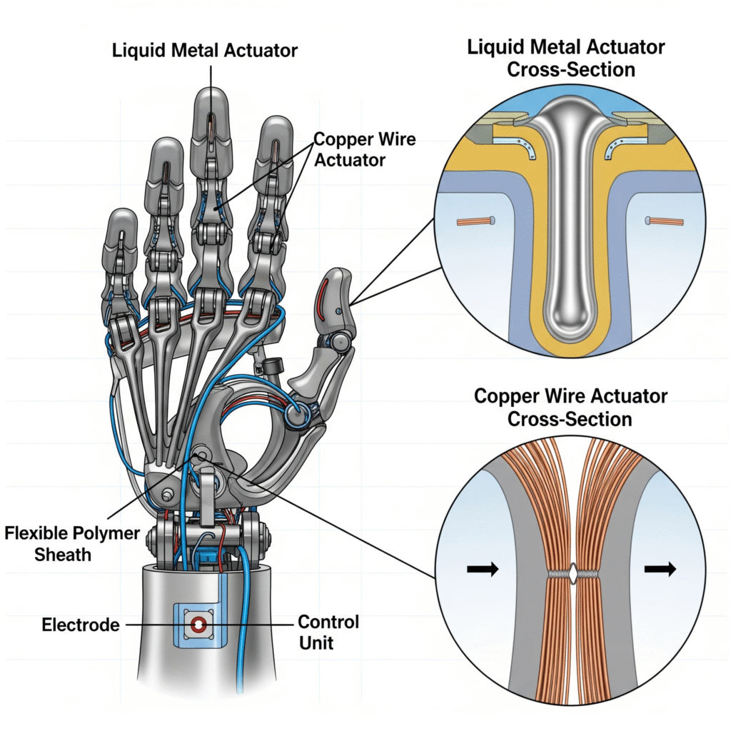
Conventional robotics relies on rigid components that move in predictable, angular motions. Gallium-based liquid metals shatter these constraints, creating machines that bend, stretch, and respond like biological systems. These materials possess exceptional surface tension (≈500 mN m⁻¹)—the highest among all liquids—opening entirely new categories of robotic movement.
Voltage-Controlled Surface Tension: Gallium droplet actuation
At just 1 volt, gallium’s surface tension changes exponentially when oxidised, disrupting the interface and creating controllable actuation mechanisms. This electrochemical control enables liquid metal actuators to achieve strain rates exceeding 1000% per second, dramatically outperforming conventional soft actuators.
Surface tension scaling provides gallium actuators with unique advantages at microscales, where forces are proportional to length (F∝L) rather than area or volume. This scaling relationship makes gallium particularly powerful in miniaturised applications where traditional actuators lose effectiveness.
Sensor-Actuator Integration: Reflexive robotic responses
The integration of sensing and actuation represents a fundamental requirement for intelligent soft robots. Gallium enables this integration through its controllable electrical properties and shape transformability. Applying voltage to a galinstan droplet causes it to penetrate porous materials, creating self-healing circuits that automatically repair disconnected wires.
This capability enables reflexive robotic responses—machines that react to environmental changes without complex programming or external control systems. The material itself becomes both sensor and actuator, simplifying robotic architecture whilst improving responsiveness.
Biomimetic Applications: Artificial muscle structures
Biomimetic artificial muscles (BMAMs) convert electrical energy into mechanical force, mimicking biological muscle operations. These structures deliver remarkable flexibility, bending capability, and stretchability whilst improving energy conversion efficiency over traditional systems. Research demonstrates maximum output forces reaching 7.81 mN, representing a 309% improvement over undoped versions.
| Property | Natural Muscle | Gallium-Based Actuator | Traditional Actuator |
|---|---|---|---|
| Response time | 30-100ms | 0.1s | Seconds to hours |
| Strain rate | ~10% s⁻¹ | >1000% s⁻¹ | <10% s⁻¹ |
| Work capacity | 40 kJ/m³ | 279 kJ/m³ | Varies widely |
The performance metrics reveal gallium actuators’ superiority in specific applications, particularly where rapid response and high strain rates are essential. Their work capacity approaches that of natural muscle whilst exceeding strain rate performance by orders of magnitude.
Key Takeaway: Gallium-based soft robotics represent a fundamental departure from rigid mechanical systems, creating machines that move, respond, and adapt with biological precision rather than mechanical predictability.
In parallel, advances in graphene applications are enabling flexible sensors, interconnects, and transparent electrodes.
Gallium Uses in Energy Storage & Conversion

Image Source: PV Magazine
Gallium’s utility extends far beyond semiconductors into energy systems where its unique properties solve critical engineering challenges across storage, thermal management, and clean fuel generation.
Gallium in Advanced Battery Systems: Lithium-thionyl chloride & specialty cells
Lithium-thionyl chloride (LiSOCl2) batteries achieve remarkable performance metrics through gallium incorporation—delivering energy densities up to 650 Wh/kg and 1280 Wh/dm³. These primary cells maintain capacity losses below 1% annually during decade-long storage periods. In commercial systems, this often works alongside graphite-based anodes and thermal paths to balance performance and stability.
Originally developed for NASA missions, this technology delivers triple the specific energy of silver-zinc alternatives—300 Wh/kg versus 100 Wh/kg. Recent research has explored gallium-based liquid metals as active battery materials, though initial studies faced challenges with corrosion in aqueous electrolytes limiting cyclic stability.
> Technical insight: Using ionic liquids shifts gallium’s redox potential, enabling stretchable batteries with up to 1400 charge-discharge cycles.
Thermal Management: CPU/GPU cooling & industrial heat transfer
Liquid gallium demonstrates exceptional heat transfer capabilities in electronic cooling systems, while graphite heat spreaders manage in-plane conductivity in compact devices.. Minichannel cooling configurations achieve heat flux dissipation up to 242 W/cm² whilst maintaining temperature rises below 50°C. Electromagnetic induction pumps generate pressure heads of 160 kPa with flow rates reaching 3.24 L/min, enabling rapid heat removal from high-performance processors.
Applied as thermal interface material, gallium-based compounds reduce contact resistance by approximately 7.77 × 10⁻³ °C/W compared to conventional thermal greases. This performance advantage stems from gallium’s superior thermal conductivity and ability to conform to surface irregularities at the microscopic level.
Safety Note: While elemental gallium is generally considered low-toxicity for casual contact, certain compounds — especially gallium arsenide (GaAs) and gallium nitride (GaN) — can release hazardous particulates during machining, recycling, or high-temperature processing, making PPE and dust-control measures essential.
Gallium also causes rapid embrittlement of aluminium and aggressively wets many metals; in cooling systems, protective coatings such as nickel/gold (Ni/Au) or polymers are recommended, and dissimilar metals should be isolated to minimise galvanic corrosion.
Hydrogen Generation: Al–Ga alloys for on-demand production
Aluminium-gallium-indium alloys provide on-demand hydrogen generation when contacted with water, addressing storage and transport limitations in hydrogen energy systems. The Al-11%Ga-3%In-1%Sn alloy achieves hydrogen conversion rates exceeding 98% across various temperature conditions.
Advanced Al-Ga-In powder preparations using melting-mechanical crushing-ball milling processes demonstrate hydrogen generation rates reaching 5337 mL·min⁻¹·g⁻¹. These reaction rates significantly outperform conventional hydrogen storage methods whilst eliminating the infrastructure requirements of compressed gas systems.
From batteries to thermal management, these diverse gallium uses illustrate the metal’s role in both high-tech and industrial energy systems.
Key Takeaway: Gallium transforms energy applications through superior thermal conductivity, enabling high-density batteries, efficient electronic cooling, and on-demand hydrogen production for next-generation clean energy systems.
Low-Melting Alloys & Thermal Applications

Image Source: Kevin Aghaei’s Lab
Gallium’s low melting point creates opportunities that extend far beyond exotic laboratory applications. The metal’s thermal properties enable practical solutions to everyday challenges, from safer medical devices to electronics that run cooler and more efficiently.
Galinstan Thermometers: Mercury-free temperature measurement
The eutectic mixture of gallium, indium, and tin (Galinstan) serves as a direct replacement for toxic mercury in clinical thermometers. Medical studies comparing measurement accuracy found no statistically significant difference between mercury and Galinstan thermometers. More importantly for clinical diagnosis, Galinstan thermometers achieved 69.2% sensitivity versus just 34.6% for digital alternatives when detecting high fevers above 39°C.
This performance advantage matters in medical settings where precise temperature measurement can influence treatment decisions. Galinstan eliminates mercury’s health risks whilst maintaining the accuracy that healthcare professionals require.
Cooling Systems: Liquid metal for electronics & industrial machinery
Electronics generate heat that limits performance and reduces component lifespan. Gallium-based liquid metals address this challenge with thermal conductivity and volumetric heat capacity that surpass both mercury and conventional cooling fluids. The performance gains are substantial:
| Cooling System | Heat Flux Capacity | Thermal Resistance |
|---|---|---|
| Water-based | <300 W/cm² | Standard baseline |
| Ga₆₈In₂₂Sn₁₀ | 1214 W/cm² | 0.077 °C/W |
| Optimised Ga-based | >1500 W/cm² | 40% lower than water |
> Technical insight: Zhang’s research team successfully demonstrated gallium-based microchannel cooling at heat fluxes exceeding 1500 W/cm².
These cooling systems enable processors and graphics cards to operate at power densities previously impossible with conventional thermal management. The result is smaller, more powerful electronics that run reliably under extreme conditions.
Gallium Mirrors & Reflective Coatings
Precision optical systems demand materials that reflect light efficiently whilst minimising noise. Gallium arsenide mirror coatings deliver at least three times reduction in mirror-related noise compared to amorphous alternatives. Their optical reflectivity also exceeds aluminium, making them valuable for solar thermal collectors and sensitive scientific instruments.
Key Takeaway: Gallium alloys enable thermal management breakthroughs — from mercury-free medical diagnostics to cooling systems that support the next generation of high-performance electronics operating at previously unattainable power densities.
Medical Imaging & Radiopharmaceuticals

Image Source: ScienceDirect.com
The same element that enables your smartphone’s connectivity has quietly become essential to detecting cancer and fighting antibiotic-resistant infections. Gallium’s radioactive isotopes possess decay properties that make them uniquely valuable for medical diagnostics, where precision can mean the difference between early detection and missed opportunities.
Gallium-67: Cancer and infection diagnostics
Gallium-67 citrate serves as a diagnostic workhorse in single-photon emission computed tomography (SPECT), particularly effective at revealing lymphomas, infections, and inflammatory conditions whilst maintaining particular relevance for imaging granulomatous reactions. The trade-off comes with its longer half-life, which results in higher radiation exposure to patients—a limitation that has driven development of more refined alternatives.
Gallium-68 PET Imaging: Targeted radiopharmaceuticals
Gallium-68 represents a significant advance in positron emission tomography (PET) with its optimal 68-minute half-life that balances imaging window with radiation exposure. 68Ga-DOTATATE has become the preferred functional imaging modality for neuroendocrine tumours across all histological grades.
The performance difference is striking: 68Ga-DOTA-TOC identified 100% of neuroendocrine tumour lesions compared to just 85% detection rates with 111In-octreotide. This superior accuracy explains why the Society for Nuclear Medicine selected 68Ga radiotracer images as ‘Image of the Year’ multiple times from 2015 onwards.
Experimental Therapeutic and Antimicrobial Uses
Beyond diagnostics, gallium compounds show unexpected promise against one of medicine’s most pressing challenges: antibiotic-resistant bacteria. Gallium nitrate disrupts bacterial iron metabolism in pathogens including Staphylococcus aureus, essentially starving bacteria of an essential nutrient they cannot do without.
Laboratory studies demonstrate tangible results: intranasal administration of gallium protoporphyrin combined with gallium nitrate significantly improved survival rates in mice with MRSA lung infections. These findings suggest gallium-based treatments could provide new weapons against superbugs that have developed resistance to conventional antibiotics.
Key Takeaway: Gallium radiopharmaceuticals represent a dual advancement in healthcare—superior diagnostic precision for cancer detection paired with emerging therapeutic potential against infections that traditional antibiotics cannot touch.
Magnetic & Specialty Industrial Uses
Gallium’s influence extends far beyond mainstream electronics, quietly enabling specialized applications across scientific research, high-performance materials, and precision manufacturing sectors.
Rare-Earth Magnet Doping: Performance enhancement in NdFeB magnets
Industrial gallium uses range from rare-earth magnet doping for performance enhancement in NdFeB magnets to niche additives in coatings and scientific instruments. Neodymium-Iron-Boron (NdFeB) magnets containing approximately 0.2% gallium represent 97% of total rare-earth magnet production.
China dominates this sector, producing 85% of all rare earth magnets with gallium consumption for NdFeB magnets exceeding 110 tonnes in 2021. Studies confirm that gallium doping significantly increases intrinsic coercivity from 12.4 kOe to 19.4 kOe while maintaining remanence.
The economics are compelling: adding just 0.5 wt% gallium delivers a 7.0 kOe coercivity improvement, outperforming equivalent amounts of expensive dysprosium or terbium doping. This cost-effective enhancement makes gallium indispensable for permanent magnet applications in wind turbines, electric vehicles, and industrial motors.
Scientific Instrumentation: Neutrino detection & particle physics tools
The Baksan Experiment on Sterile Transitions (BEST) utilises 47 metric tonnes of liquid gallium metal to detect neutrinos through the reaction 71Ga(νe,e)71Ge. When neutrinos interact with gallium-71 nuclei, they convert gallium into germanium-71, which scientists extract and count to measure neutrino flux.
This application demonstrates gallium’s role in fundamental physics research, where its nuclear properties enable detection of some of the universe’s most elusive particles.
Environmental Tracers: Oceanography and climate studies
Gallium serves as an environmental tracer in oceanographic research, helping scientists track water movements and climate patterns. Its unique geochemical signature allows researchers to trace oceanic circulation patterns and understand long-term climate changes.
Niche Industrial Additives: Ski wax, specialty coatings
Japanese company GALLIUM WAX produces high-performance ski waxes containing metallic gallium alongside fluorocarbons. These products create superior glide characteristics by altering water droplet configuration, reducing friction between ski bases and snow.
The precision required in competitive skiing—where milliseconds matter—showcases gallium’s ability to deliver performance advantages in the most demanding applications.
Key Takeaway: From enabling breakthrough physics experiments to enhancing Olympic-level athletic performance, gallium’s specialized applications demonstrate how even small quantities of strategic materials can drive innovation across diverse technological frontiers.
Global Supply Chain & India’s Strategic Context

Image Source: CSIS
Behind gallium’s ubiquity in modern electronics lies a stark geopolitical reality: China controls nearly 80% of global gallium production with 498 tonnes of annual capacity,maintaining its 97–98% global market share as of 2024 creating one of the most concentrated supply chains in critical materials.
This dominance isn’t accidental. Gallium exists primarily as a by-product of bauxite and zinc processing, with concentrations of just 1 part per million in Earth’s crust. China’s control over these upstream industries translates directly into gallium market power, leaving Japan (72 tonnes), South Korea, Russia, and Germany fighting over the remaining scraps.
Global Production Landscape: China’s dominance & alternatives
The numbers tell a sobering story of strategic dependency. Export restrictions imposed by China since 2022 have sent shockwaves through global technology supply chains, forcing countries to confront their vulnerability in securing this critical element essential for modern electronics.
| Country | Production Capacity (tonnes) | % of Global Supply |
|---|---|---|
| China | 498 | ~80% |
| Japan | 72 | ~12% |
| Others | 53 | ~8% |
Strategic insight: With global tech manufacturing dependent on just three countries for gallium supply, even minor disruptions create cascading effects across semiconductors, telecommunications, and defence industries.
Recycling & Resource Recovery: Technical challenges & innovations
Despite improving techniques, recycling contributes a mere 10-15% of global gallium supply. Recovery methods remain complex, relying on precipitation and solvent extraction processes that struggle with economic viability at current volumes. This limited recycling capacity amplifies dependence on primary production—and China’s chokehold.
The most common recovery streams include Bayer process liquor from alumina refining and GaAs wafer scrap from semiconductor fabs. While technically feasible, low gallium content and fluctuating market prices often make recovery economically challenging unless coupled with high-value byproducts.
India’s Gallium Capabilities: NALCO production & semiconductor policies
National Aluminium Company (NALCO) operates India’s sole gallium production facility—a 50 tonnes per annum plant in Odisha operational since 2013. While modest compared to Chinese capacity, this domestic production provides crucial strategic advantage as India pursues semiconductor self-reliance through its national semiconductor mission.
NALCO’s facility processes gallium from bauxite residue, demonstrating how India can extract strategic value from existing mining operations. Yet at 50 tonnes annually, domestic production covers only a fraction of India’s growing gallium requirements for 5G infrastructure, defence electronics, and emerging semiconductor manufacturing.
Strategic Risk Assessment: Supply security & policy measures
The gallium supply chain represents a textbook case of strategic vulnerability. Countries worldwide now prioritise developing alternative sources, stockpiling strategies, and recycling capabilities to reduce dependence on Chinese production. Australia, Canada, and several African nations possess untapped gallium potential, but developing these sources requires years of investment and infrastructure development.
For India, the path forward demands balancing immediate import needs with long-term supply security. Expanding NALCO’s capacity, developing gallium recovery from electronic waste, and securing international partnerships represent critical components of a comprehensive strategy.
Policy levers such as Production-Linked Incentives (PLI) for compound semiconductors, integration with the National Semiconductor Mission, and partnerships in gallium nitride device manufacturing could enable India to capture higher-value nodes in the gallium supply chain—moving beyond raw material production into finished semiconductor components.
Key Takeaway: China’s stranglehold on gallium production creates both immediate risks and long-term opportunities for countries willing to invest in alternative supply chains, recycling capabilities, and strategic stockpiles of this critical element essential for modern electronics.
Manufacturing Challenges & Commercialisation
Converting gallium from promising laboratory demonstrations to reliable industrial production presents formidable obstacles that mirror the element’s complex nature.
Technical Barriers: Oxide layer management & fabrication precision
Gallium’s tendency to form an oxide ‘skin’ within seconds of air exposure creates the most persistent manufacturing challenge. This protective layer, whilst useful for flexible electronics, disrupts precision fabrication processes where uniform geometries are essential. The oxide interferes with consistent shapes and dimensions, making reproducible manufacturing difficult to achieve.
Gallium oxide crystals compound these difficulties through their inherent brittleness. Grinding and machining operations frequently result in fractures or micro-cracks unless processing conditions are meticulously controlled. These limitations become more pronounced in ultra-wide bandgap Ga₂O₃ semiconductor production.
Thermal management presents another significant hurdle. Ga₂O₃’s low thermal conductivity causes localised heating near junction regions, potentially triggering premature device failure. Whilst heterogeneous integration offers a pathway forward, lattice mismatch between different substrate materials continues to limit progress.
Scaling from Lab to Industry: Cost, yield & infrastructure needs
Production economics face substantial pressure from expensive iridium crucibles required for gallium oxide processing. These crucibles, essential for withstanding extreme temperatures without contaminating the material, demand frequent replacement and have seen dramatic price increases. The cost impact extends throughout the supply chain, making large-scale production economically challenging.
| Manufacturing Challenge | Impact on Commercialisation | Potential Solution |
|---|---|---|
| Oxide skin formation | Inconsistent geometries | Dip-coating in NaOH |
| Iridium crucible costs | Higher production expenses | Alternative materials research |
| Limited wafer size | Reduced industrial adoption | Scaling to 150-200mm wafers |
Silicon semiconductor development requires minimal teams and capital investment, but gallium-based technologies demand substantially greater resources, creating inherent investor risk. Foundry availability compounds these challenges, with most facilities concentrated in Asia. Locating pure-play foundries capable of low-volume, specialised production alongside recruiting skilled personnel presents ongoing obstacles.
Case Study: Carnegie Mellon’s wearable gallium sensor project
Researchers at Carnegie Mellon University addressed gallium’s oxide formation challenge through an innovative SMAW-DC (Selective Metal-Alloy Wetting with Dip Coating) method. The process employs a sodium hydroxide bath that removes oxide skin when patterned wafers are dipped into the solution. Controlling withdrawal speed enables repeatable liquid metal geometries compatible with established lithographic processes.
This approach demonstrates how targeted engineering solutions can overcome gallium’s inherent processing difficulties, providing a pathway from laboratory concept to manufactureable device.
Key Takeaway: Manufacturing gallium-based technologies demands sophisticated process control and substantial capital investment, yet innovative approaches are successfully bridging the gap between laboratory potential and industrial reality.
Future Applications & Technology Roadmap
From a metal Mendeleev once only predicted to a material enabling satellites, 5G, and wearable medical devices, gallium’s journey is a lesson in how materials science reshapes industries. Melting at body temperature yet stable at extreme heat, gallium powers high-frequency semiconductors, flexible electronics, solar cells, and advanced medical imaging.
Its compounds — GaAs, GaN, and Ga₂O₃ — outperform silicon in speed, efficiency, and durability, driving innovations from space-grade photovoltaics to 6G communications. Flexible circuits, self-healing electronics, and gallium-68 diagnostics highlight how it enables entirely new technology categories.
But supply is fragile. China produces ~80% of the world’s gallium, and extraction as a bauxite/zinc byproduct limits scale. India’s 50-tonne output offers a foothold but falls short of semiconductor demand.
The next decade’s growth in telecom, EVs, aerospace, and quantum computing will intensify demand. Nations that diversify supply, invest in recycling, and advance fabrication will gain a decisive edge.
Key Takeaway: Gallium is no longer obscure — it’s a strategic resource at the heart of tomorrow’s electronics, energy systems, and defence technologies. Secure supply means secure leadership in the next wave of industrial progress.
FAQs
What makes gallium unique among metals?
Gallium has the largest liquid temperature range of any element, melting at just 29.76°C but not boiling until around 2400°C. It also forms a protective oxide skin when exposed to air, enabling unique applications in flexible electronics.
How is gallium used in solar technology?
Gallium is used in high-efficiency solar cells, particularly gallium arsenide (GaAs) cells for space applications. It’s also a key component in CIGS (copper indium gallium selenide) thin-film solar cells and can be used as a dopant to improve silicon solar cell performance.
What role does gallium play in modern electronics?
Gallium compounds like gallium arsenide (GaAs) and gallium nitride (GaN) are crucial in creating high-speed, high-frequency semiconductors used in smartphones, WiFi devices, and 5G infrastructure. These materials offer superior performance to traditional silicon in many applications.
Are there any medical applications for gallium?
Yes, gallium isotopes are used in medical imaging. Gallium-67 is used for detecting certain cancers and infections, while Gallium-68 is used in PET scans, particularly for imaging neuroendocrine tumours. Some gallium compounds also show promise as antimicrobial agents.
What challenges exist in gallium production and supply?
China currently dominates global gallium production, controlling about 80% of supply. This concentration creates potential supply chain vulnerabilities. Additionally, gallium is primarily obtained as a byproduct of aluminium and zinc processing, which can limit production flexibility.



![The Surprising Truth About Beryllium Applications in Modern Technology [2025 Guide]](https://ik.imagekit.io/lxsotwajc/wpmedia/wp-content/uploads/2025/06/featured-Image3-440x264.webp)