Last Updated on September 15, 2025 by Hemanth
Table of Contents
🔎 30-Second Summary
From smartphones and laptops to automotive dashboards and life-saving medical monitors, a soft, nearly invisible metal forms the backbone of the touch-responsive, vibrant displays that define modern life: indium.
Despite making up just 0.05 parts per million of Earth’s crust, as scarce as silver — indium remains one of the least recognised elements driving technological progress. With no primary mining and production concentrated in a few countries, indium is classified as a critical mineral, making its scarcity and unique properties indispensable to the digital economy and renewable energy transition.
Around 70% of global indium uses flow into producing indium tin oxide (ITO), the invisible foundation that transforms glass into responsive touchscreens and efficient solar cells. Engineers call it an “alloy vitamin” because microscopic quantities transform entire material properties, turning ordinary metals into high-performance components. These traits place indium at the heart of technological revolutions in renewable energy, 5G communications, advanced semiconductors, and precision manufacturing.
Scratch indium metal with your fingernail — it yields like butter. This extraordinary softness might suggest weakness, yet this silvery element quietly powers the touchscreen in your pocket, the solar panels on rooftops, and the precision electronics that define our digital age.
You won’t find indium listed on product specifications, but you’ve almost certainly held it today. Hidden inside smartphone displays, laptop screens, and flat-panel televisions, this rare metal enables the transparent conductive coatings that make modern electronics possible.
That versatility comes from indium’s unusual chemistry. Found naturally combined with zinc, iron, lead, and copper ores rather than existing alone, this post-transition metal requires sophisticated extraction processes that few countries have mastered. Its strategic importance comes not from abundance, but from unique properties that remain largely unmatched by substitutes.
Indium bridges the visible and invisible worlds of technology — conducting electricity while staying transparent, remaining pliable at extreme temperatures, and enabling photons to become electrons in ways silicon cannot.
Atomic & Chemical Foundations of Indium
“We believe that materials science changes the world.” — Greg Evans, CEO, Indium Corporation
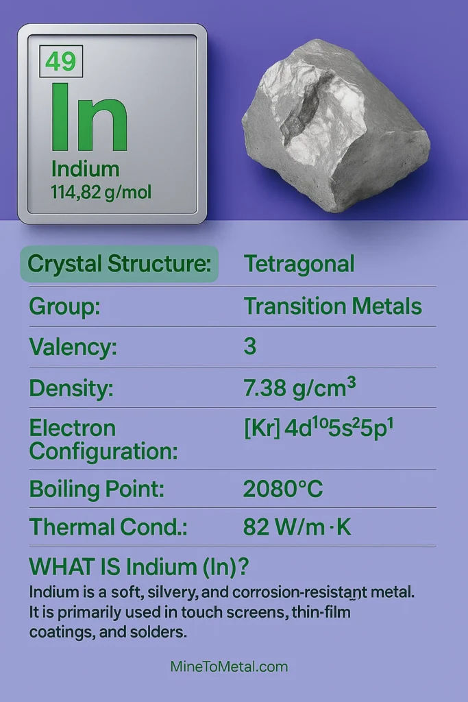
Indium (chemical symbol In, atomic number 49) may occupy an unremarkable position in the periodic table’s fifth period, but its atomic structure creates a metal with genuinely exceptional characteristics. This post-transition metal exhibits such extreme malleability that it registers just 1.2 on the Mohs hardness scale — softer than lead, softer than tin, yielding to fingernails and kitchen knives alike.
Yet this apparent weakness masks chemical versatility that drives billion-dollar industries.
Physical traits: softness, melting point, reflectivity vs tin/lead
Indium announces its presence acoustically. When bent, it produces a distinctive high-pitched “cry” — a crackling sound created by crystal twinning as atomic layers shift against each other. This audible signature resembles tin’s famous “tin cry,” but indium’s version carries a sharper pitch that engineers use as an informal quality test.
Beyond sound, indium exhibits an unusual affinity for glass surfaces. Like gallium, it possesses the rare ability to “wet” glass — spreading across surfaces and adhering where most metals would bead up. This property proves critical in applications requiring intimate contact between metal and substrate.
The element’s thermal behaviour defines its utility. With a melting point of 156.60°C, indium liquefies at temperatures achievable with boiling water and modest heating. Its boiling point, however, reaches 2080°C — creating an extraordinarily wide liquid range that spans nearly 2000°C. This thermal window enables applications from cryogenic seals to high-temperature processes.
Comparison of Physical Properties
| Melting Point | 156.6 °C | 231.9 °C | 327.5 °C | Indium melts with boiling water heat, ideal for low-temp solders. |
| Density | 7.31 g/cm³ | 7.29 g/cm³ | 11.3 g/cm³ | Nearly as light as tin, far lighter than dense lead. |
| Mohs Hardness | 1.2 | 1.5 | 1.5 | Soft enough to yield under a fingernail. |
| Special Traits | High reflectivity, “cry” when bent, wets glass | “Tin cry” when bent | High density, shielding properties | Unusual quirks define indium’s unique role. |
Indium’s optical properties rival precious metals. Its exceptional reflectivity approaches silver’s performance while resisting the tarnishing that degrades silver mirrors over time. This combination of optical excellence and chemical stability makes it valuable for specialized mirror applications requiring long-term reliability.
Valency and oxidation states (+1, +3)
Indium’s electron configuration [Kr]4d¹⁰5s²5p¹ provides three electrons available for chemical bonding, yet its behaviour defies simple predictions. The element readily adopts +3 oxidation states in most stable compounds, losing all three outer electrons to achieve a stable configuration.
More intriguingly, indium also forms +1 compounds, particularly among halides and specialized materials. This dual oxidation behaviour positions indium between gallium (strongly favouring +3) and thallium (preferring +1), creating unique chemical flexibility. The stabilization of the +1 state results from the “inert pair effect” — a relativistic phenomenon where the 5s electrons become increasingly difficult to remove.
This oxidation state flexibility translates directly into material properties. Indium(III) compounds remain chemically stable and non-oxidizing, while many indium(I) compounds function as powerful reducing agents — enabling diverse applications from electronics to catalysis.
Stable vs radioactive isotopes (113, 115)
Indium presents one of chemistry’s most unusual isotopic profiles. Among the 39 known isotopes spanning masses from 97 to 135, natural indium consists almost entirely of a radioactive isotope — a rarity shared only with tellurium and rhenium.
The isotopic composition reveals this anomaly:
- Indium-113: The only stable isotope, representing merely 4.28% of natural indium
- Indium-115: A radioactive isotope with a half-life of 4.41×10¹⁴ years, comprising 95.72% of natural indium
Indium-115’s radioactivity poses no practical concerns — its half-life exceeds the universe’s age by four orders of magnitude. For medical applications, artificial indium-111 proves more useful with its 2.8-day half-life, ideal for radiotracer studies.
Organoindium compounds in organic synthesis
Indium’s chemical versatility extends into organic chemistry through organoindium compounds featuring indium-carbon bonds. Most exist as In(III) derivatives, though cyclopentadienylindium(I) represents a notable In(I) exception.
Trimethylindium stands as the most significant organoindium compound, serving as a critical precursor for semiconductor materials. These compounds enable indium-mediated allylation reactions that proceed in water without organic solvents or promoters — a remarkable synthetic advantage.
The appeal extends beyond convenience. Indium exhibits no known toxicity while maintaining stability in air and water at room temperature. These characteristics position organoindium reagents as attractive alternatives for single electron transfer processes where traditional metals require harsh conditions.
Key Takeaway: Indium’s atomic structure creates a unique combination of extreme softness, dual oxidation chemistry, and thermal versatility that enables applications impossible with conventional metals — from transparent conductors to specialized alloys and synthetic chemistry.
Indium in Consumer Electronics and Display Technologies

From smartphones and laptops to automotive dashboards and life-saving medical monitors, a soft, nearly invisible metal underpins modern interactive displays: indium. This article explores the essential indium uses that shape modern electronics and beyond
Every swipe on a screen relies on indium uses most people never see. Indium forms indium tin oxide (ITO)—a transparent, conductive film that lets touch sensors read your finger while keeping displays bright and sharp. ITO has historically consumed over 70% of global indium and remains the metal’s leading end use, making this one of the most important indium uses in consumer technology.”
The Paradox of Indium Tin Oxide (ITO): Conducting Electricity, Staying Transparent
ITO marries two traits that rarely coexist: low sheet resistance for fast, accurate touch response and high visible transmittance so colours stay vivid. Commercial films are tuned into application-specific bands—typically ~10–100 Ω/ at ~80–90% transmittance, by adjusting thickness and deposition. Modern phones use single- or double-ITO touch sensors, and many integrate additional ITO electrodes within the display stack.
A single smartphone display may contain multiple indium tin oxide layers, sometimes up to four, each engineered to balance transparency with electrical performance (USGS, 2023). If this balance shifts too far, either touch responsiveness slows due to high resistance or display brightness suffers from reduced transmittance, making precise tuning essential.
Beyond phones, the same properties power automotive displays, aerospace control panels, and medical monitoring devices where transparency and conductivity must coexist.
Key Properties of ITO: The Balancing Act
| Property | Typical Value/Range | Why It Matters |
|---|---|---|
| Electrical resistivity | ~1×10⁻⁴ Ω·cm | Enables rapid, stable signal conduction |
| Optical transmittance (visible) | ~80–90% | Maintains clear, bright visuals |
| Sheet resistance | ~10–100 Ω/□ | Supports small to large (even flexible) displays |
Engineering trade-off: lowering resistance generally reduces transmittance; manufacturing tunes films to hit the right balance for each device and form factor. Most applications require films achieving less than 20 ohms per square resistance whilst maintaining optical transmittance exceeding 80%.
Broad Applications of ITO: Beyond the Smartphone
ITO’s versatility turns glass and plastics into high-function surfaces while staying transparent:
- LCD panels: Acts as the transparent pixel/common electrode deposited by sputtering; uniform sheet resistance enables high-resolution control of liquid-crystal alignment and light transmission.
- OLED displays: Serves as the anode/transparent electrode, supporting hole injection and high optical transmittance so colours and brightness are preserved in thin, efficient stacks.
- Touchscreens: Patterned ITO grids power self/mutual-capacitive sensing; low resistance keeps latency down while maintaining clarity, core to responsive, multi-touch UX.
- Smart windows: ITO-based electrochromic/low-E coatings modulate visible light and infrared heat, improving building energy efficiency without blocking views.
- Infrared reflectors: Tailored ITO films reflect thermal IR but pass visible light, aiding thermal management in displays, optics, and architectural glass.
Also used for EMI/RFI shielding, antistatic coatings, photovoltaics (as a TCO front contact), and electroluminescent lighting, broadening the footprint of indium applications beyond consumer screens.
Case Study: Samsung Display technology
Samsung Display revolutionized screen technology by developing quantum dot displays free of hazardous cadmium, leveraging indium phosphide-based quantum dots with innovative triple-layer protective coatings. Launched in 2015, these TVs matched traditional cadmium-based displays in performance and guaranteed over a decade of reliable service. This breakthrough not only enhanced colour and brightness but also significantly reduced toxic substance use in millions of households worldwide.
Health and Safety in ITO Manufacturing
While indium in finished devices is stable and non-toxic, manufacturing and recycling environments present very different risks. Occupational studies have shown that chronic exposure to indium-tin oxide (ITO) dust can cause respiratory diseases, sometimes referred to as “indium lung.” Regulatory agencies in Japan, the United States, and Europe have since introduced stricter exposure limits and monitoring guidelines. Ensuring safe workplace practices and designing recycling streams that minimize dust release are now essential parts of sustaining indium’s role in global electronics.
ITO Alternatives and Substitution Research
Although indium tin oxide remains the industry standard for transparent conductors, research into substitutes is accelerating. Graphene films, silver nanowires, and conductive polymers are among the most promising candidates, offering high transparency with tunable conductivity. While none yet match ITO’s performance-to-cost balance at scale, these alternatives reflect growing industry interest in reducing reliance on scarce critical minerals like indium.
Key Takeaway: Indium’s simultaneous transparency and conductivity remain unmatched at commercial scale. Despite ongoing efforts to develop alternatives, no substitute currently delivers ITO’s combined properties with equivalent performance and cost-effectiveness.
Semiconductors & Optoelectronics
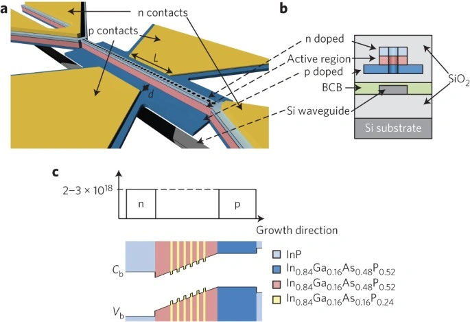
Image Source: Nature
Forget silicon’s limitations — indium compounds rewrite the rules of semiconductor physics. Where silicon struggles with light emission and high-frequency signals, indium-based materials excel, creating pathways for photons and electrons that conventional semiconductors simply cannot match.
Indium phosphide (InP) in 5G and photonics
Indium phosphide stands as the foundation material powering next-generation 5G networks and integrated photonics. This III-V compound semiconductor enables high-frequency microelectronic components that handle signals above 100 GHz — frequencies where silicon-based devices falter.
The critical advantage stems from InP’s direct bandgap property, which allows efficient light emission. Silicon lacks this capability entirely, creating an insurmountable barrier for optoelectronic integration.
“InP technology has left behind its status as merely promising and is showing viability in commercial environments with applications from optical fibre connections to free-space communication.”
Monolithic indium phosphide-based optoelectronic integrated circuits (OEICs) convert optical signals directly into radio signals in advanced 5G systems, eliminating the bottleneck between optical and radio networks. Processing speeds reach 50 times faster than electronic counterparts, enabling the seamless data flow that 5G promises demand.
Indium gallium arsenide in laser diodes and detectors
Indium gallium arsenide (InGaAs) dominates infrared detection between 1 and 1.7 μm wavelengths for measurable reasons. Matched to indium phosphide substrates, InGaAs delivers a 0.75 eV bandgap with electron mobility approaching 10,000 cm²/V·s at room temperature — specifications that outperform germanium, silicon, and other detector materials.
Performance advantages include:
- 100% internal quantum efficiency — effectively perfect light-to-electron conversion
- Lower dark current across equivalent sensor areas
- Faster response times compared to germanium alternatives
InGaAs serves as the active medium in semiconductor lasers across multiple wavelengths: 905 nm, 980 nm, 1060 nm, and 1300 nm. InGaAs/AlInAs quantum cascade lasers operate at room temperature within the 3-8 μm range, enabling applications from atmospheric monitoring to industrial process control.
Activated indium in transistor doping, gas sensors and device fabrication
Indium doping transforms semiconductor performance through precise electronic modification. Indium-doped SnO₂ gas sensors demonstrate four times higher sensitivity toward methanol compared to undoped versions. This enhancement improves selectivity while preventing particle agglomeration and enabling lower-temperature operation.
Indium antimonide and arsenide for infrared and quantum devices
Indium antimonide (InSb) functions as a direct bandgap semiconductor with a 0.17 eV energy gap at room temperature, optimised for middle-wave infrared imaging up to 5.5 μm wavelengths. InSb possesses the highest ambient-temperature electron mobility (78,000 cm²/V·s) among all known semiconductors except carbon nanotubes.
Quantum confinement in InSb nanowires creates unique optoelectronic properties by reducing dark current through size reduction and phonon scattering suppression. This enables photodetectors to maintain performance whilst operating at higher temperatures — a crucial advantage for practical deployment.
Table: Indium compounds vs applications
| Compound | Bandgap | Key Properties | Applications |
|---|---|---|---|
| InP | Direct | High electron velocity, direct bandgap | 5G communications, photonic chips, OEICs |
| InGaAs | 0.75 eV | High quantum efficiency, fast response | Infrared detectors, laser diodes, quantum cascade lasers |
| InSb | 0.17 eV | Highest electron mobility, infrared sensitivity | Thermal imaging, FLIR systems, quantum wells |
| In-doped SnO₂ | Varies | Enhanced sensitivity, lower operating temperature | Gas sensors, surface acoustic wave devices |
Key Takeaway: Indium compounds enable the convergence of electronics and photonics, creating communication systems that process information at light speed and detection systems sensitive enough to identify individual photons.
Solar Energy & Photovoltaics
“Indium alloys can be used for the production of solar cells.” — Refractory Metals and Alloys Editorial Team, Industry publication specialising in advanced materials
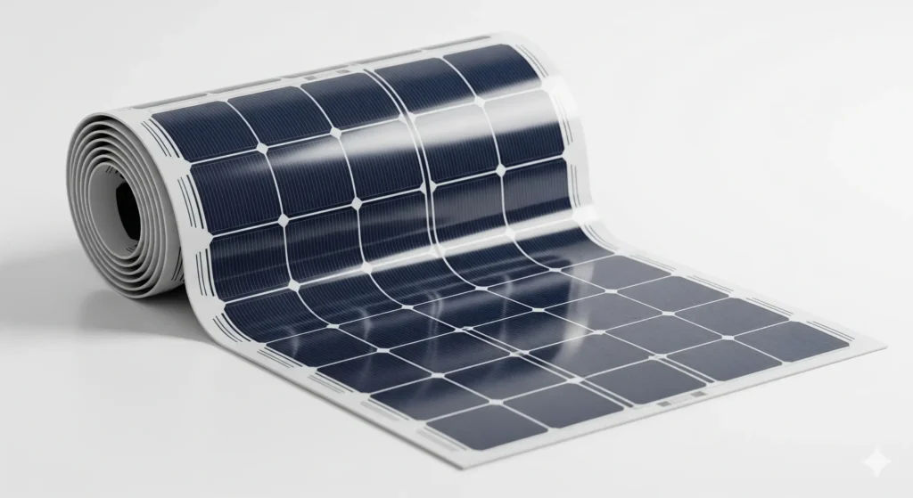
Image Source: EnergySage
Indium’s influence extends far beyond touchscreens into solar energy systems that challenge conventional photovoltaic design. The element enables thin-film technologies that outperform silicon panels in specific conditions while using dramatically less material.
Copper Indium Gallium Selenide (CIGS) thin-film solar cells
CIGS represents a different approach to solar energy capture. These cells deposit semiconductor layers of copper, indium, gallium, and selenide onto glass, plastic, or metal substrates using just 1-2 micrometres of thickness — a fraction of conventional silicon requirements.
The manufacturing process builds layers through co-evaporation or precursor reaction methods, followed by chemical-bath deposition of cadmium sulphide and zinc oxide. This heterojunction structure differs fundamentally from silicon’s homojunction design, enabling direct bandgap properties that absorb light more efficiently per unit thickness.
CIGS requires only 1% of the semiconductor material needed in traditional silicon cells, yet maintains commercial efficiency levels between 13-18% compared to silicon’s 20-25% peak performance.
Efficiency under low-light vs silicon panels
Performance comparisons reveal CIGS advantages in real-world conditions rather than laboratory peaks.
| Parameter | CIGS Panels | Silicon Panels | Real-World Impact |
|---|---|---|---|
| Commercial Efficiency | 13-18% | 20-25% | Silicon higher in ideal conditions |
| Low-Light Performance | Maintains efficiency | Significant drop | CIGS superior in cloudy conditions |
| Temperature Coefficient | -0.36%/°C | Typically -0.4% to -0.5%/°C | CIGS better in heat |
| Annual Power Generation | 126.14 kWh/m² | 118.26 kWh/m² | CIGS produces ~7% more energy |
Field studies of comparable installations show CIGS glass-aluminium panels achieving 74% performance ratio versus 70% for crystalline silicon under identical 2.2× concentration factors. This advantage stems from CIGS maintaining efficiency during partial shading and temperature fluctuations.
Role in next-generation lightweight solar panels
CIGS flexibility enables solar applications impossible with rigid silicon panels. Deposition onto polymer foils creates:
- Building-integrated photovoltaics (BIPV): Solar tiles and facades that integrate architecturally
- Portable systems: Rollable chargers for military and emergency applications
- Vehicle integration: Curved installations on cars, boats, and aircraft
- Space applications: Lightweight panels for satellites and space stations
Swiss Federal Laboratories achieved record 20.4% efficiency with CIGS on flexible polymer substrates, proving flexible doesn’t mean compromised performance. The technology’s exceptional radiation tolerance makes it particularly valuable for space applications where silicon degrades more rapidly.
Case Study: Building-Integrated CIGS Challenge: Generate solar power without disrupting architectural aesthetics Solution: CIGS adapted for solar shingles and building materials that match conventional construction Results: Buildings maintain visual appeal while generating renewable energy Impact: Solar adoption in locations where traditional panels violate building codes or aesthetic requirements
Key Takeaway: CIGS technology positions indium at the centre of flexible solar systems that generate more annual energy than silicon despite lower peak efficiency — proving that real-world performance matters more than laboratory specifications.
Alloys, Solders & Thermal Interfaces
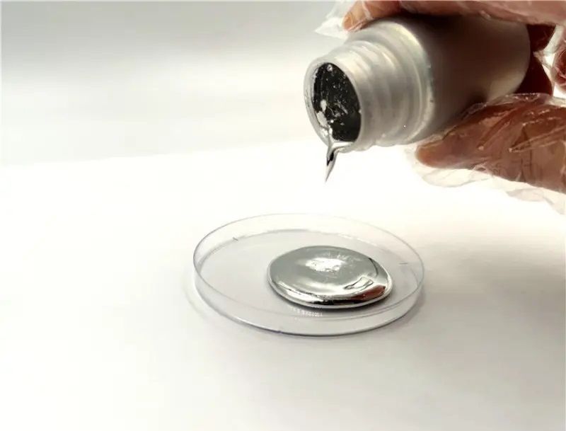
Image Source: Indium Corporation
Indium’s malleability creates opportunities where other metals fail catastrophically. At temperatures that would crack conventional solders or render standard sealing materials useless, indium-based alloys maintain their integrity, enabling precision electronics and extreme-environment applications that demand absolute reliability.
Low-temperature solders for precision electronics (including Indium 30 uses)
One of the most valuable indium uses is in low-temperature solders, heat-sensitive components demand soldering solutions that won’t destroy what they’re meant to connect. Pure indium melts at 157°C, significantly below tin-lead alternatives that typically require 183-220°C processing temperatures. This temperature reduction prevents thermal damage to delicate semiconductor devices, optical components, and advanced ceramics.
Indium accommodates thermal expansion mismatches between dissimilar materials — a critical advantage when bonding glass to metal or ceramic to semiconductor substrates. Where rigid solders crack under thermal cycling, indium-based joints absorb stress through controlled deformation.
Specialised indium alloy compositions target specific performance requirements:
- Pure indium (In100): 157°C melting point, bonds glass, ceramics, and quartz
- Indium-silver (In97/Ag3): Enhanced strength with 143°C melting point
- Indium-tin (In52/Sn48): Ultra-low 118°C eutectic for extreme heat sensitivity
Galinstan as a mercury substitute
Another category of indium uses is in Galinstan, an alloy comprising of gallium, indium, and tin — remains liquid at -19°C, creating a non-toxic alternative to mercury in applications requiring liquid metal properties. This alloy eliminates mercury’s toxicity concerns while maintaining essential liquid metal characteristics.
Commercial Galinstan contains proprietary additives that improve flowability and reduce surface tension, though it’s not technically a eutectic composition.
| Property | Galinstan | Mercury | Performance Advantage |
|---|---|---|---|
| Toxicity | Minimal | Highly toxic | Safe handling |
| Melting Point | -19°C | -38.8°C | Room temperature liquid |
| Density | 6.44 g/cm³ | 13.53 g/cm³ | Reduced weight |
| Environmental Impact | Negligible | Severe | Simplified disposal |
Applications include precision thermometers, liquid-mirror telescopes, thermal interfaces for high-performance computing, and heat exchangers operating across extreme temperature ranges.
Indium foils and gaskets in cryogenics and aerospace
Cryogenic temperatures and ultra-high vacuum environments destroy conventional sealing materials through brittleness, outgassing, or thermal contraction failures. Indium’s exceptional ductility enables hermetic seals that function reliably from room temperature down to liquid helium conditions.
During installation, indium conforms to microscopic surface imperfections, creating leak-tight seals with contact pressures as low as 1-5 MPa — far below the 20-50 MPa required by conventional gasket materials. These seals form mechanically without heat application, preventing thermal stress to sensitive equipment.
Critical performance characteristics include:
- Ductility retention: Maintains flexibility at -269°C (liquid helium temperature)
- Chemical stability: Resists corrosion from aggressive gases and cryogenic fluids
- Low vapour pressure: 10⁻¹⁰ Torr at room temperature, essential for vacuum applications
- Thermal cycling endurance: Withstands repeated temperature excursions without seal failure
These properties make indium sealing solutions indispensable in superconducting magnet assemblies, particle accelerators, space-based instruments, and cryogenic research equipment where failure isn’t an option.
Key Takeaway: Indium enables joining and sealing solutions in conditions where conventional materials fail — from ultra-low temperatures to precision electronics assembly — making it essential for applications demanding absolute reliability under extreme conditions.
Medical & Nuclear Applications
Beyond touchscreens and solar cells, indium serves medicine and nuclear energy in ways that directly impact human health and safety. These applications demand exceptional precision and reliability — qualities that indium’s unique nuclear and chemical properties deliver consistently.
Indium-111 in white blood cell tagging and tumour detection
Indium-111, with its 2.80-day half-life, functions as a precision radiotracer in nuclear medicine. This radioisotope decays by electron capture to cadmium-111, emitting detectable gamma radiation at 173 keV (89%) and 247 keV (94%).
The isotope’s half-life creates an ideal diagnostic window — long enough for comprehensive imaging procedures yet short enough to limit patient radiation exposure. Once Indium-111 labels white blood cells, these tagged cells accumulate at infection or inflammation sites when reinjected.
Medical professionals use this technique for:
- Identifying hidden infections
- Evaluating inflammatory disease
- Detecting abdominal abscesses
- Diagnosing prosthetic joint infections
Indium-111 also binds to tumour-targeting agents including monoclonal antibodies and peptides. The somatostatin receptor binding peptide pentetreotide (OctreoScan) labelled with Indium-111 effectively identifies various neuroendocrine tumours.
Dental and medical implant alloys
Dental applications have incorporated indium for over two decades. During porcelain-fused-metal procedures, indium creates an oxide film that bonds metal and porcelain together.
Dental alloys containing 5-10% indium demonstrate:
- Improved bond strength with porcelain
- Enhanced tarnish resistance
- Superior corrosion resistance
Ti-In binary alloys show mechanical strength and hardness comparable to commercially pure titanium while maintaining similar corrosion resistance.
Neutron capture alloys (Ag-In-Cd rods) in nuclear reactors
Indium’s high neutron-capture cross-section for thermal neutrons makes it essential for nuclear reactor control rods. These safety-critical components typically contain 80% silver, 15% indium, and 5% cadmium (AIC).
Control rods regulate reactor power by absorbing neutrons. They can be partially inserted during normal operation or fully inserted for emergency shutdown. Under neutron bombardment, indium transmutes into tin while silver converts to cadmium. This transformation eventually creates a hexagonal compact phase that occupies more volume than the original cubic phase, causing volumetric expansion.
Key Takeaway: Indium’s precision in medicine enables doctors to visualise hidden disease processes, while its neutron absorption properties provide critical safety systems in nuclear reactors, demonstrating how this element operates at the intersection of healing and protection.
Emerging Smart Materials & Coatings
Indium’s chemical flexibility positions it at the forefront of materials innovation, where laboratory breakthroughs transition into practical solutions for challenges that seemed impossible just years ago.
YInMn blue pigment for durable coatings
YInMn blue, discovered serendipitously by researchers at Oregon State University, contains yttrium, indium, manganese, and oxygen. This remarkable pigment delivers superior durability and chemical resistance compared to conventional blue colorants. Its infrared radiation reflection properties make it particularly valuable for energy-saving cool coatings that reduce building temperatures. When ignited, YInMn blue burns with a distinctive violet flame—a signature of indium atoms in action.
The pigment addresses a centuries-old challenge: creating stable blue colours that resist fading under UV exposure and chemical attack. Traditional blue pigments often contain toxic materials or degrade over time, but YInMn blue maintains its vibrancy while offering thermal management benefits that conventional colours cannot match.
Smart windows and infrared filters
Indium tin oxide coatings enable smart windows that dynamically adjust heat and light transmission based on environmental conditions. These systems control building temperature and energy consumption, contributing to more sustainable built environments. Infrared-shielding films prepared by dispersing ITO nanoparticles in silica matrices achieve complete IR radiation blocking at wavelengths above 1400 nm while maintaining over 80% transparency in the visible spectrum.
These applications demonstrate indium’s ability to manipulate electromagnetic radiation selectively—blocking unwanted heat while allowing useful light to pass through, a property that enables responsive building materials.
Speciality catalysts: Indium chloride in organic synthesis
Indium trichloride serves as an exceptional catalyst due to its moisture compatibility and stability in aqueous media. Its non-toxicity, abundance, and recyclability make InCl₃ highly valuable for synthesising heterocyclic compounds with excellent chemo- and regioselectivity.
Unlike many traditional catalysts that require anhydrous conditions and inert atmospheres, indium trichloride operates effectively in water-based systems, simplifying reaction setups and reducing environmental impact.
Quantum devices
Indium functions as a high-cooling-power nuclear refrigerant for quantum nanoelectronics. Graphene quantum dots sandwiched between polymethylsilsesquioxane layers create indium-free nonvolatile memory devices with ON/OFF ratios as large as 10⁴ and cycling endurance exceeding 10⁴ seconds.
These applications showcase indium’s role in quantum technologies, where precise control over electronic and thermal properties becomes critical for device functionality.
Flexible electronics
Eutectic indium-gallium alloy (EGaIn) containing 75.5% gallium and 24.5% indium enables thermally conductive elastomers for stretchable electronics. This liquid metal maintains electrical conductivity while changing form, creating circuits with rubber-like elasticity alongside metal-like thermal properties.
EGaIn represents a paradigm shift in electronics design—components that bend, stretch, and deform while maintaining electrical functionality, opening possibilities for wearable devices and conformable sensors.
Key Takeaway: Indium’s unique properties unlock next-generation materials spanning durable pigments, responsive building components, and quantum devices—demonstrating how this element continues driving innovation across diverse technological frontiers where conventional materials reach their limits.
Supply, Recycling & Global Criticality
Indium’s supply story reveals a dependency web that most technology companies prefer not to discuss. This element follows an unusual path from ore to application — one that creates strategic vulnerabilities hiding beneath every touchscreen and solar panel.
Indium as a by-product of zinc mining
Indium exists as a passenger element, never forming deposits rich enough for primary mining. Instead, it emerges as a by-product from zinc-sulphide ores, specifically sphalerite. Approximately 95% comes from zinc production, with the remaining derived from tin (4%) and copper (1%).
This dependency creates a fundamental disconnect between indium demand and supply control. Zinc miners extract indium not because markets need it, but because zinc production happens to yield it. The extraction yield from zinc-lead ores ranges between 70-90%, yet only about 35% of indium in zinc reaches refineries capable of extracting it. The element sits more abundant in Earth’s crust than silver, but accessing it requires zinc mining infrastructure and specialised recovery technology.
In practice, indium first accumulates in the flue dusts of zinc smelters. These residues are leached and purified through hydrometallurgical techniques such as solvent extraction and precipitation. Final refining often involves electrolysis, yielding high-purity indium metal suited for demanding electronic and optoelectronic applications.
Recycling from display glass and electronics
Electronic waste represents an indium goldmine that remains largely untapped. LCD panels contain up to three times more indium than natural ores. Recycling metals requires 2-10 times less energy compared to primary extraction.
“Urban mining of electronics represents an untapped indium reservoir hiding in plain sight.”
Yet proper e-waste recycling faces significant obstacles. Current recovery rates reach 43% in Europe, merely 12% in Asia, and 10% in the Americas. Most discarded displays end up in landfills rather than recovery facilities, creating both environmental hazards and resource waste. The technical challenge lies in separating microscopic ITO layers from glass substrates without contamination — a process requiring sophisticated chemical recovery techniques.
Top global producers: China, South Korea, Canada
Geographic concentration defines indium’s strategic risk profile:
| Country | Annual Production | Global Share |
|---|---|---|
| China | 760 tonnes (2024) | ~70% |
| South Korea | 200 tonnes | ~10% |
| Japan | 64 tonnes | ~6% |
| Canada | 55 tonnes | ~5% |
Top global producers: China, South Korea, Canada
Geographic concentration defines indium’s strategic risk profile:
| Country | Annual Production | Global Share |
|---|---|---|
| China | 760 tonnes (2024) | ~70% |
| South Korea | 200 tonnes | ~10% |
| Japan | 64 tonnes | ~6% |
| Canada | 55 tonnes | ~5% |
According to the U.S. Geological Survey, global refined indium production is roughly 800 tonnes per year, a remarkably small volume compared to base metals like copper or aluminum.
China’s dominance stems from its zinc refining capacity and willingness to invest in indium recovery infrastructure. This concentration creates potential supply disruptions that could affect global electronics manufacturing, particularly given indium’s limited substitutability in critical applications.
Criticality index and limits on substitution
Demand for indium is projected to increase by 231% by 2050 compared to 2018 levels. The electronics sector drives this growth through expanding touchscreen markets, 5G infrastructure deployment, and thin-film solar adoption.
Substitutes exist — including antimony tin oxide coatings, carbon nanotubes, and silver nanowires — yet none match indium’s combined properties at commercial scale. Silver nanowires offer conductivity but cost significantly more. Carbon nanotubes show promise but remain difficult to manufacture consistently. Graphene electrodes attract research interest but face processing challenges that prevent mass production.
The substitution gap widens in high-performance applications where indium’s unique combination of transparency, conductivity, and processing compatibility remains unmatched.
Key Takeaway: Indium’s by-product nature and concentrated production create a strategic bottleneck that grows more critical as digital technologies expand — making recovery from electronic waste not just environmentally sensible, but strategically essential.
India’s Indium Landscape
Image Source: Machine Maker
India faces a stark reality with indium: complete import dependence for a metal that powers the very technologies driving its digital transformation ambitions. While the country positions itself as a global electronics manufacturing hub, it lacks domestic access to this critical element that enables touchscreens, solar panels, and advanced semiconductors.
Indium Recovery Efforts at Hindustan Zinc
Hindustan Zinc Limited represents India’s most promising pathway to domestic indium supply. As the country’s largest zinc producer, the company has initiated laboratory-scale indium recovery from its zinc processing waste streams at the Chanderiya smelter complex in Rajasthan. These efforts target the microscopic quantities of indium typically discarded during conventional zinc refining.
The technical challenge lies in extracting commercially viable quantities from waste streams that contain indium at concentrations often below 0.01%. Early-stage pilot programs focus on hydrometallurgical processes that could potentially yield several tonnes annually — modest by global standards, yet strategically significant for reducing import vulnerability.
Research Institutions: BARC, C-MET
| Institution | Research Focus | Strategic Significance |
|---|---|---|
| BARC | Indium radioisotopes, semiconductor materials | Medical diagnostics, defence electronics autonomy |
| C-MET | Indium recovery techniques, e-waste processing | Circular economy, sustainable sourcing |
The Bhabha Atomic Research Centre develops indigenous capabilities for indium-111 production, crucial for nuclear medicine applications where import restrictions could affect patient care. Meanwhile, the Centre for Materials for Electronics Technology pursues urban mining techniques to recover indium from electronic waste — a potentially significant domestic resource given India’s growing e-waste generation.
Current research focuses on establishing purification protocols that meet international standards for electronics-grade indium, where impurity levels must remain below 10 parts per million for semiconductor applications.
Strategic Opportunities in Solar, Defence, and Electronics Sectors
India’s “Make in India” initiative identifies indium as essential for achieving manufacturing self-reliance in three critical sectors. The country’s 500 GW renewable energy target by 2030 depends partly on thin-film solar technologies that require indium compounds. Similarly, indigenous defence electronics production — from radar systems to precision targeting equipment — relies on indium-based semiconductors.
The strategic calculus is clear: India’s technology sovereignty ambitions collide with complete import dependence for a metal that China controls approximately 70% of global refined production. This dependency extends beyond direct military applications to the civilian technologies that underpin economic competitiveness.
Key Takeaway: India’s indium landscape embodies the broader challenge of critical mineral security — balancing immediate import needs against long-term strategic autonomy.
With no primary production capacity, recycling and recovery from zinc smelter residues and electronic waste remain the only viable pathways to reduce dependence and build future supply security.
Toxicity, Safety & Environmental Impact
Indium enables remarkable technologies, but its industrial handling presents serious occupational health risks that regulatory bodies worldwide are still learning to address.
Indium lung and occupational exposure risks
Indium lung disease, first documented in 2003, represents a severe occupational hazard for workers in ITO production facilities. This potentially fatal condition causes pulmonary alveolar proteinosis that may progress to fibrosis, with or without emphysema. The disease continues advancing even after exposure ends, frequently resulting in pneumothorax or respiratory failure.
Workers in ITO manufacturing face the highest risk. Sandblasters cleaning ITO production machinery show serum indium levels reaching 149 μg/L — dramatically elevated compared to background levels. The progression from exposure to clinical symptoms can take years, making early detection challenging.
Toxicity comparison: Indium metal vs indium tin oxide
| Form | Toxicity Level | Primary Concern | Exposure Route |
|---|---|---|---|
| Indium Metal | Lower | Minimal when solid | Inhalation of dust/fume |
| Indium Tin Oxide | Higher | Severe lung effects | Respiratory exposure |
Pure indium metal poses minimal risks in bulk form unless processed into dust or fumes. The real danger lies in ITO nanoparticles, which can penetrate deep into lung tissue and trigger inflammatory responses that persist long after initial exposure.
Global regulatory exposure limits and safety measures
Regulatory responses vary significantly across regions. Japan established the most stringent limits at 3×10⁻⁴ mg/m³ following several worker fatalities. OSHA maintains a considerably higher threshold of 0.1 mg/m³, reflecting ongoing debates about appropriate exposure standards.
Essential protection measures include local exhaust ventilation, respiratory equipment rated for nanoparticle filtration, and regular medical monitoring focused on lung function assessment. Companies now implement biological monitoring programs tracking serum indium levels in high-risk workers.
The contrast is stark: while indium enables the digital devices we use daily, the workers who produce these components face significant health risks that only stringent safety protocols can mitigate.
Key Takeaway: Indium’s technological value comes with serious occupational health trade-offs, requiring continuous vigilance in industrial settings where worker safety protocols can mean the difference between technological progress and irreversible lung damage.
Conclusion
Indium stands out not for its abundance, but for how critical even trace amounts become in enabling modern technology. This exploration reveals a metal whose strategic importance far exceeds its visibility — powering touchscreens, enabling 5G communications, and facilitating solar energy capture while remaining largely unknown outside specialized industries.
The element’s unique combination of transparency and conductivity in ITO form has fundamentally altered human-device interaction. Its semiconductor compounds process photonic signals at unprecedented speeds, while its malleability enables precision applications impossible with conventional materials. These properties position indium at the intersection of multiple technological revolutions that define our digital age.
Yet indium’s strategic value comes with significant vulnerabilities. As a byproduct of zinc processing, supply remains concentrated in few countries, creating geopolitical dependencies for technologies increasingly central to economic competitiveness. Projected demand growth of 231% by 2050 amplifies these concerns, particularly as substitutes fail to match indium’s combined properties at commercial scale.
The health implications of indium processing — notably “indium lung disease” in workers — underscore the complex trade-offs between technological advancement and human safety. These challenges demand rigorous safety protocols and highlight the hidden costs of materials that enable modern conveniences.
For countries like India, indium represents both opportunity and strategic vulnerability. While domestic recovery initiatives at Hindustan Zinc and research at BARC and C-MET show promise, the gap between technological ambitions and material security remains substantial. The path forward requires balancing import dependencies against building indigenous capabilities across the entire value chain.
Indium exemplifies how seemingly obscure elements often prove foundational to civilizational progress. Despite lacking the recognition of gold or the ubiquity of aluminium, this soft metal quietly enables the devices, communications networks, and energy systems that define contemporary life. Its scarcity ensures that mastering indium’s supply chain will increasingly determine which nations lead in critical technologies.
As digital infrastructure expands and renewable energy deployment accelerates, indium’s strategic importance will only grow. The countries and companies that secure reliable access to this “alloy vitamin” while developing sustainable processing capabilities will hold significant advantages in the technological competitions ahead.
FAQs
What are the primary industrial applications of indium?
Indium is predominantly used in the production of flat-panel displays as indium tin oxide (ITO), a transparent and conductive coating for glass. It’s also crucial in semiconductor manufacturing and low-melting-point metal alloys for solders and vacuum seals.
How does indium feature in our daily lives?
Indium is present in many everyday devices through indium tin oxide (ITO), which is essential for touch screens, flatscreen TVs, and solar panels. Its ability to conduct electricity while remaining transparent makes it invaluable in these technologies.
What unique properties make indium valuable for electronics?
Indium has several distinctive traits: it ‘screams’ when bent, has a low melting point of about 156.6°C, and serves as an excellent thermal interface material. These properties make it ideal for various electronic applications, including cryogenic systems.
How is indium utilised in television technology?
Indium is a crucial component in nearly all flat screen TVs, including LCD, LED, and OLED models. The transparent conductive layer created by indium tin oxide (ITO) allows electrical signals to pass across the screen while maintaining visual clarity.
What role does indium play in renewable energy technologies?
Indium is a key element in the production of thin-film solar cells, particularly in Copper Indium Gallium Selenide (CIGS) technology. These solar cells are known for their efficiency, flexibility, and ability to perform well in low-light conditions, making indium essential for advancing solar energy adoption.